- 您现在的位置:买卖IC网 > Sheet目录1992 > CY2SSTV857ZXI-32 (Silicon Laboratories Inc)IC CLK DDR266/333BUF1:10 48TSSOP
CY2SSTV857
.......................... Document #: 38-07557 Rev. *E Page 4 of 8
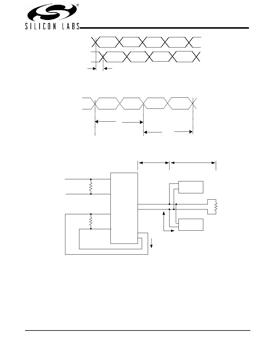
CLKIN
t
pd
Yx or FBIN
Figure 2. Propagation Delay Time tPLH, tPHL
t
C(n+1)
Yx
t
C(n)
Figure 3. Cycle-to-cycle Jitter
PLL
FBIN
FBIN#
120
Ohm
120
Ohm
CLK
CLK#
DDR -
SDRAM
120
Ohm
VTR
VCP
0.3"
= 2.5"
= 0.6" (Split to Terminator)
DDR _SDRAM
represents a capacitive load
DDR -
SDRAM
FBOUT#
FBOUT
Output load capacitance for 2 DDR-SDRAM Loads: 5 pF< CL< 8 pF
Figure 4. Clock Structure # 1
发布紧急采购,3分钟左右您将得到回复。
相关PDF资料
CY505YC64DT
IC CLK CK505 BROADWATER 64TSSOP
CYW150OXC
IC CLOCK 440BX AGP 56SSOP
CYW173SXC
IC CLK GEN TAPE DRV 4CH 16SOIC
CYW305OXC
IC CLOCK W305 SOLANO 56SSOP
DAC5674IPHPG4
IC DAC 14BIT 400MSPS 48-HTQFP
DAC7621EBG4
IC SNGL 12BIT PARALLEL D/A 20SSO
DAC7801KPG4
IC DUAL 12BIT CMOS DAC 24-DIP
DAC8043AESZ
IC DAC 12BIT MULT SRL INP 8SOIC
相关代理商/技术参数
CY2SSTV857ZXI-32T
功能描述:时钟缓冲器 2.5V 60-200MHz 1:10 Diff DDR266/333 B/D RoHS:否 制造商:Texas Instruments 输出端数量:5 最大输入频率:40 MHz 传播延迟(最大值): 电源电压-最大:3.45 V 电源电压-最小:2.375 V 最大功率耗散: 最大工作温度:+ 85 C 最小工作温度:- 40 C 封装 / 箱体:LLP-24 封装:Reel
CY2V012FLXCT
制造商:Cypress Semiconductor 功能描述:
CY2V013FLXCT
功能描述:锁相环 - PLL IC XTAL OSC VOLT RoHS:否 制造商:Silicon Labs 类型:PLL Clock Multiplier 电路数量:1 最大输入频率:710 MHz 最小输入频率:0.002 MHz 输出频率范围:0.002 MHz to 808 MHz 电源电压-最大:3.63 V 电源电压-最小:1.71 V 最大工作温度:+ 85 C 最小工作温度:- 40 C 封装 / 箱体:QFN-36 封装:Tray
CY2V013FLXIT
功能描述:锁相环 - PLL FleXo HiPerf ClkGen RoHS:否 制造商:Silicon Labs 类型:PLL Clock Multiplier 电路数量:1 最大输入频率:710 MHz 最小输入频率:0.002 MHz 输出频率范围:0.002 MHz to 808 MHz 电源电压-最大:3.63 V 电源电压-最小:1.71 V 最大工作温度:+ 85 C 最小工作温度:- 40 C 封装 / 箱体:QFN-36 封装:Tray
CY2V014FLXCT
功能描述:锁相环 - PLL IC XTAL OSC VOLT RoHS:否 制造商:Silicon Labs 类型:PLL Clock Multiplier 电路数量:1 最大输入频率:710 MHz 最小输入频率:0.002 MHz 输出频率范围:0.002 MHz to 808 MHz 电源电压-最大:3.63 V 电源电压-最小:1.71 V 最大工作温度:+ 85 C 最小工作温度:- 40 C 封装 / 箱体:QFN-36 封装:Tray
CY2V014FLXIT
功能描述:锁相环 - PLL FleXo HiPerf ClkGen RoHS:否 制造商:Silicon Labs 类型:PLL Clock Multiplier 电路数量:1 最大输入频率:710 MHz 最小输入频率:0.002 MHz 输出频率范围:0.002 MHz to 808 MHz 电源电压-最大:3.63 V 电源电压-最小:1.71 V 最大工作温度:+ 85 C 最小工作温度:- 40 C 封装 / 箱体:QFN-36 封装:Tray
CY2V995
制造商:CYPRESS 制造商全称:Cypress Semiconductor 功能描述:S2.5/3.3V 200-MHz Multi-Output Zero Delay Buffer
CY2V9950
制造商:CYPRESS 制造商全称:Cypress Semiconductor 功能描述:2.5/3.3V 200-MHz Multi-Output Zero Delay Buffer